
One of the most challenging aspects of the optical inspection system in materials research is its resolution and speed. A high-speed, super-resolution optical system can make this possible. Jade Mat is an advanced optical system that can image the region of interest (ROI) at high speed. Spectral acquisition can occur simultaneously with image acquisition, which will be very useful for materials research. It is a non-destructive imaging technique that can be used to preserve the material structure and characteristics of sensitive and precious samples. With this process, complete 3-D material signals can be obtained with a high degree of accuracy. Our core value is its super resolution optical technology, which surpasses traditional optics. Our aims to improve the resolution to 100nm or 50nm to overcome the limitations of AFMs, spectroscopic microscopes, and even electron microscopes.
Applications in Nanomaterials research
As compared to other high-end imaging techniques, optical imaging of nanomaterials has a great deal of limitations, especially for 2-D materials like graphene. With its ultrahigh speed spectral mapping and high-speed optical imaging, our system stands out because of its accuracy in measuring micro areas. It features automatic light path switching, auto-focus, rapid identification of the layers of 2-D materials, and laser micro-area annealing/modification. Software for spectral image analysis includes wavelength, intensity, half-height width, band image and overlay, statistical analysis of spectral information, etc. This can be upgraded with advanced OAMs and other functional modules to expand the development space of cutting-edge materials research.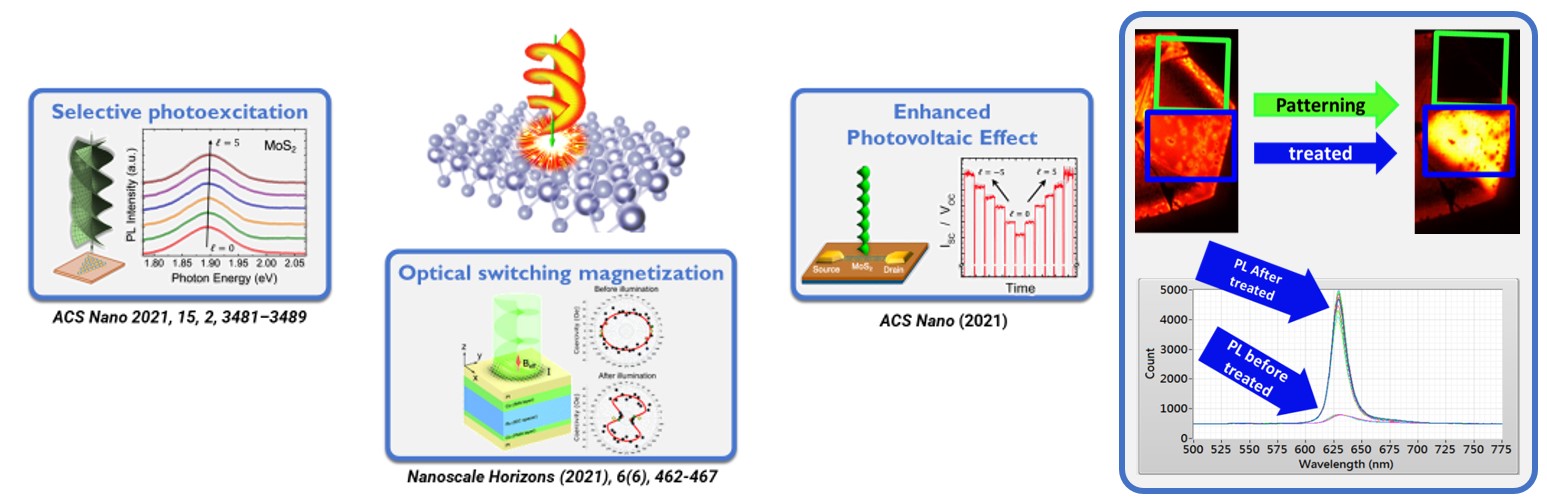 Applications in Semiconductor research
Our newly developed compound semiconductor inspection modules can provide extremely rapid and accurate defect information by detecting lattice structures such as 3C, 4H, and 6H, dislocations, and three-dimensional stress distributions of a sample using fast 3-D Raman. This means that overall detection and analysis of compound semiconductors is possible even for 3-D defects and stresses.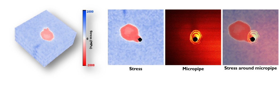 Application in Perovskite
This model is the best system for detecting perovskites due to its high speed and resolution in crystal gain spectral images. The instrument has a non-destructive spectrum measurement mode with high photoelectric efficiency and one-step detection. Additionally, light patch switching is fully automatic, as well as automatic focusing and 3-D depth perception. Furthermore, the system is able to provide fluorescent and white light imaging, fluorescence spectrum, Raman spectrum mapping, transient spectrum (TRPL), FLIM can be used in magnetic fields and provides the best environmental control at various temperatures.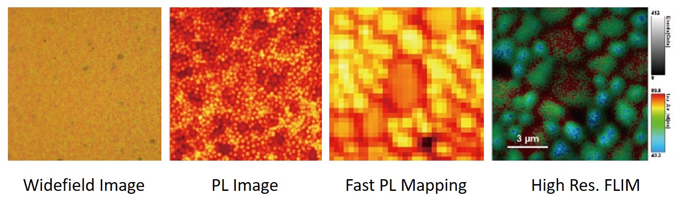 Applications in Micro LED study
In order to evaluate epitaxial uniformity and mass transfer quality, it is most effective to implement a Micro LED based optical inspection system using sub-micron spatial analysis and sub-nano spectral analysis. The epitaxy inspection includes bow/warp, wavelength, intensity, half-height width, dominant wavelength, reflectivity, and film thickness. A crystal grain inspection includes peak wavelength, peak intensity, half-height width, and dominant wavelength, as well as an analysis of CIE XY panel. The items of inspection are EL yields and inter-layer defects. The P-EL detection method does not require spot measurements in order to predict EL lighting status. That is the key to Micro LED automated mass inspection.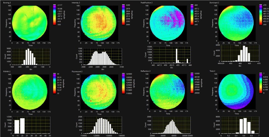
| Applications in Quantum Dot Inspection
The system customized for quantum dot detection is non-destructive and can provide high-resolution fluorescent images that can detect quantum dots quickly. In order to achieve fast alignment, it will be possible to switch between adjacent quantum dots and match the spectrum modules using a very fast light positioning method. Thus, various parameters can be analyzed with accuracy, speed, and synchronization. |
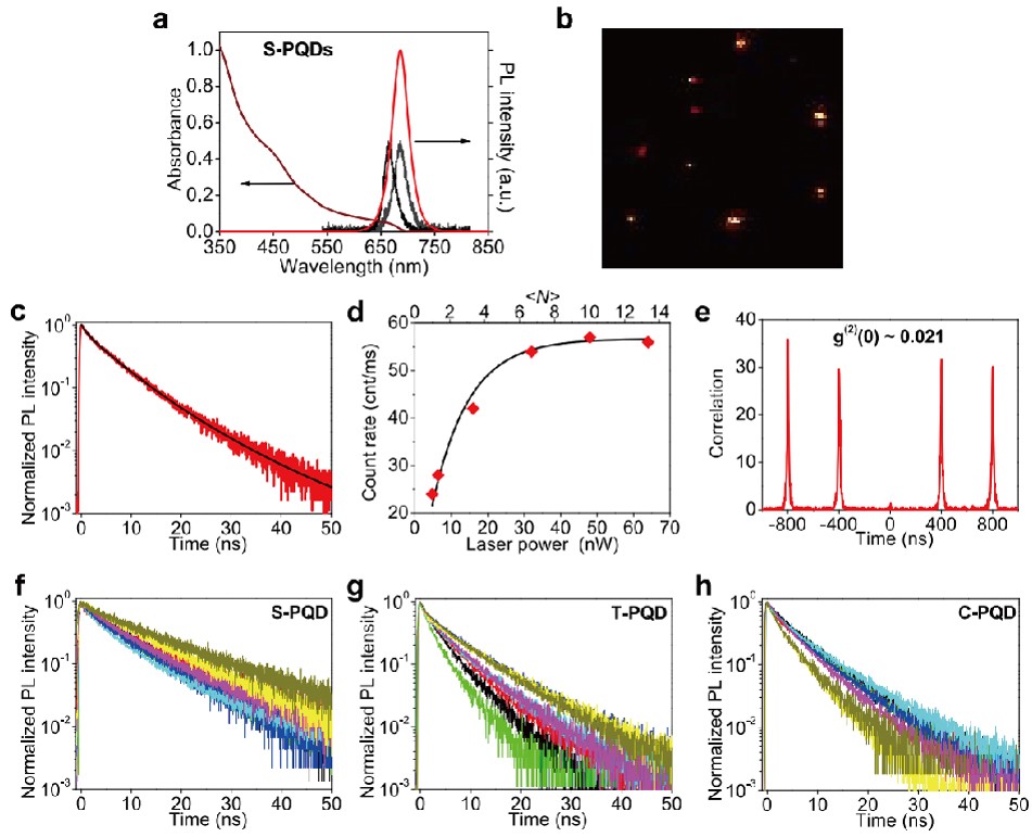 |
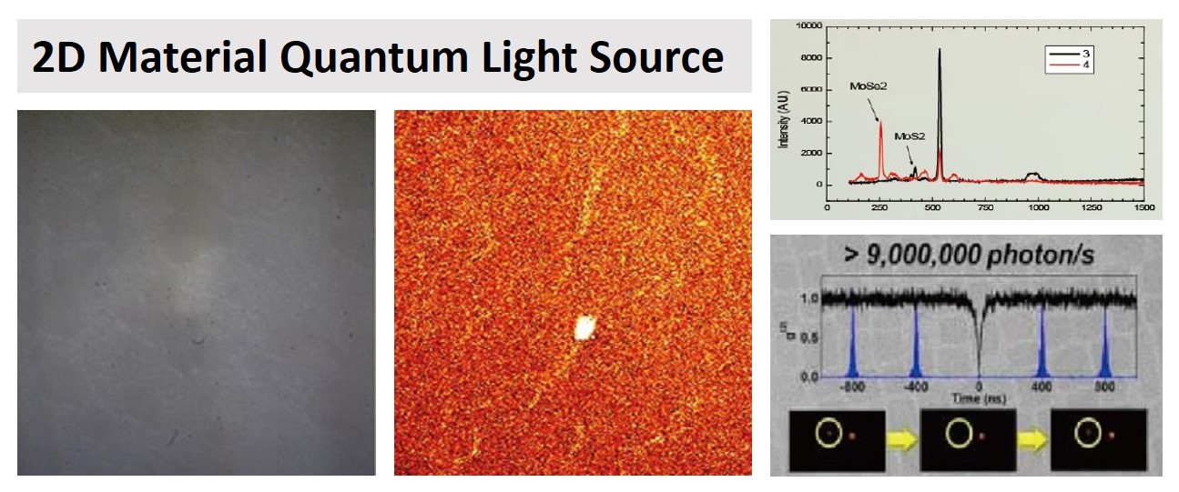
Application in Single-Photon Source Detection
The best solution for detecting Quantum Emitter material properties is to use clear images and accurately positioned optics. The quantum light source is capable of focusing quickly on its luminous core and it can be directly measured qualitatively and quantitatively with the high-sensitivity, low-noise single-photon detection module. This enables quantum technology research to be easily upgraded.
 |
Written by: Meera Kanakamma Mohan |
Related Product:

5D digital optical microscope: Advanced Materials Series |
5D digital optical microscope: Surface Science Series |