 |
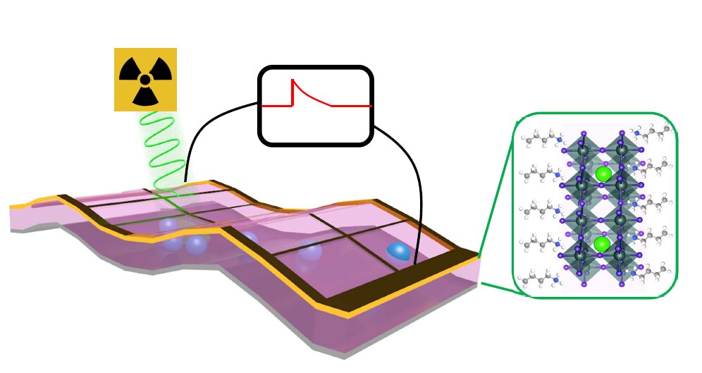
| X-ray detectors made with 2-dimensional perovskite thin films convert X-ray photons to electrical signals without requiring an outside power source, and are a hundred times more sensitive than conventional detectors. Credit: Los Alamos National Laboratory |
A new X-ray detector prototype is on the brink of revolutionizing medical imaging, with dramatic reduction in radiation exposure and the associated health risks, while also boosting resolution in security scanners and research applications, thanks to a collaboration between Los Alamos National Laboratory and Argonne National Laboratory researchers.
Solid-state radiation detectors, using crystalline semiconductors to convert radiation photons to electrical charges, outperform other technologies with high detectivity and sensitivity. The researchers demonstrate a thin-film x-ray detector comprised with highly crystalline two-dimensional Ruddlesden-Popper phase layered perovskites fabricated in a fully depleted p–i-n architecture.
“The perovskite material at the heart of our detector prototype can be produced with low-cost fabrication techniques,” said Hsinhan (Dave) Tsai, an Oppenheimer Postdoctoral fellow at Los Alamos National Laboratory. “The result is a cost-effective, highly sensitive, and self-powered detector that could radically improve existing X-ray detectors, and potentially lead to a host of unforeseen applications.”
The detector replaces silicon-based technology with a structure built around a thin film of the mineral perovskite, resulting in a hundred times more sensitivity than conventional silicon-based detectors. In addition, the new perovskite detector does not require an outside power source to produce electrical signals in response to X-rays. This detector shows high diode resistivity of 1012 ohm·cm in reverse-bias regime leading to a high x-ray detecting sensitivity up to 0.276 C Gyair−1 cm−3. Such high signal is collected by the built-in potential underpinning operation of primary photocurrent device with robust operation. The detectors generate substantial x-ray photon–induced open-circuit voltages that offer an alternative detecting mechanism. This findings suggest a new generation of x-ray detectors based on low-cost layered perovskite thin films for future x-ray imaging technologies.
High sensitivity perovskite detectors could enable dental and medical images that require a tiny fraction of the exposure that accompanies conventional X-ray imaging. Reduced exposure decreases risks for patients and medical staff alike. The fact that perovskite detectors can be made very thin allows them to offer increased resolution for highly detailed images, which will lead to improved medical evaluations and diagnoses. Lower-energy and increased-resolution detectors could also revolutionize security scanners and imaging in X-ray research applications.
Because perovskite is rich in heavy elements, such as lead and iodine, X-rays that easily pass through silicon undetected are more readily absorbed, and detected, in perovskite. As a result, perovskite significantly outperforms silicon, particularly at detecting high-energy X-rays. This is a crucial advantage when it comes to monitoring X-rays at high-energy research facilities, such as synchrotron light sources.
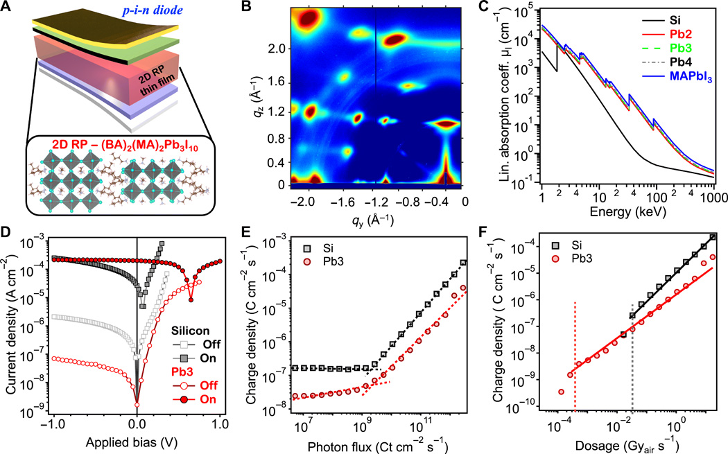 |
Thin-film x-ray detectors and their properties.
(A) Schematic illustration of the 2D RP–based p–i–n thin-film x-ray detector device architecture composed of (BA)2(MA)2Pb3I10 (dubbed as Pb3) as an absorbing layer. (B) GIWAXS map of the 2D RP thin film done under synchrotron beam. (C) Calculated linear x-ray absorption coefficient (μl) as a function of incident radiation energy for hybrid perovskite materials and silicon. (D) J–V characteristic for 2D RP and silicon reference devices in the dark and under x-ray (10.91 keV) exposure. (E) X-ray–generated charge density as a function of x-ray dosage for 2D RP (red) and silicon diode (black) under zero bias. (F) X-ray–induced charge density subtracted by the dark noise (signal-to-noise ratio) for 2D RP and silicon reference detector from (E). |
Perovskite films can be deposited on surfaces by spraying solutions that cure and leave thin layers of the material behind as a result, the thin-layer detectors will be much easier and cheaper to produce than silicon-based detectors, which require high-temperature metal deposition under vacuum conditions.
“Potentially, we could use ink-jet types of systems to print large scale detectors,” said Tsai. “This would allow us to replace half-million-dollar silicon detector arrays with inexpensive, higher-resolution perovskite alternatives.”
In addition to the promise of thin-layer perovskites in X-ray detectors, thicker layers work well provided they include a small voltage source. This suggests that their useful energy range could be extended beyond X-rays to low-energy gamma-rays.
The study is published in Science Advances.
Reference:
- https://phys.org/news/2020-04-self-powered-x-ray-detector-revolutionize-imaging.html
- https://advances.sciencemag.org/content/6/15/eaay0815