 |
|
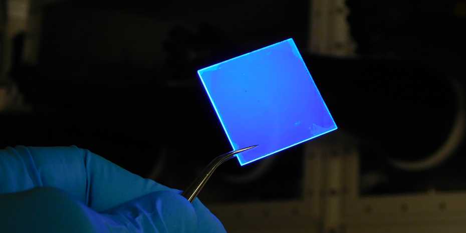
UV light shines on a pane of glass, coated with several layers of two-dimensional semiconductor nanoplatelets, which emits blue light. (Photograph: ETH Zurich / Jakub Jagielski)
|
ETH scientists have further developed QLED technology for screens. They have produced light sources that for the first time emit high-intensity light in only one direction. This reduces scattering losses, which makes the technology extremely energy efficient.
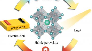
Miniaturized photonic sources based on semiconducting two-dimensional (2D) materials offer new technological opportunities beyond the modern III-V platforms. For example, the quantum-confined 2D electronic structure aligns the exciton transition dipole moment parallel to the surface plane, thereby outcoupling more light to air which gives rise to high-efficiency quantum optics and electroluminescent devices. It requires scalable materials and processes to create the decoupled multi-quantum-well superlattices, in which individual 2D material layers are isolated by atomically thin quantum barriers. Here, we report decoupled multi-quantum-well superlattices comprised of the colloidal quantum wells of lead halide perovskites, with unprecedentedly ultrathin quantum barriers that screen interlayer interactions within the range of 6.5 Å. Crystallographic and 2D k-space spectroscopic analysis reveals that the transition dipole moment orientation of bright excitons in the superlattices is predominantly in-plane and independent of stacking layer and quantum barrier thickness, confirming interlayer decoupling.
Stacked and insulated from each other
Chih-Jen Shih, Professor of Technical Chemistry at ETH Zurich, and his team of researchers have now stacked extremely thin (2.4 manometers) semiconductor platelets in such a way that they are separated from each other by an even thinner (0.65 manometer) insulating layer of organic molecules. This layer prevents quantum-physical interactions, which means that the platelets emit light predominantly in only one direction, even when stacked.
“The more platelets we pile on top of each other, the more intense the light becomes. This lets us influence the light intensity without losing the preferred direction of emission,” says Jakub Jagielski, a doctoral student in Shih’s group and first author of the study published in Nature Communications. That is how the scientists managed to produce a material that for the first time emits high-intensity light in only one direction.
 |
|
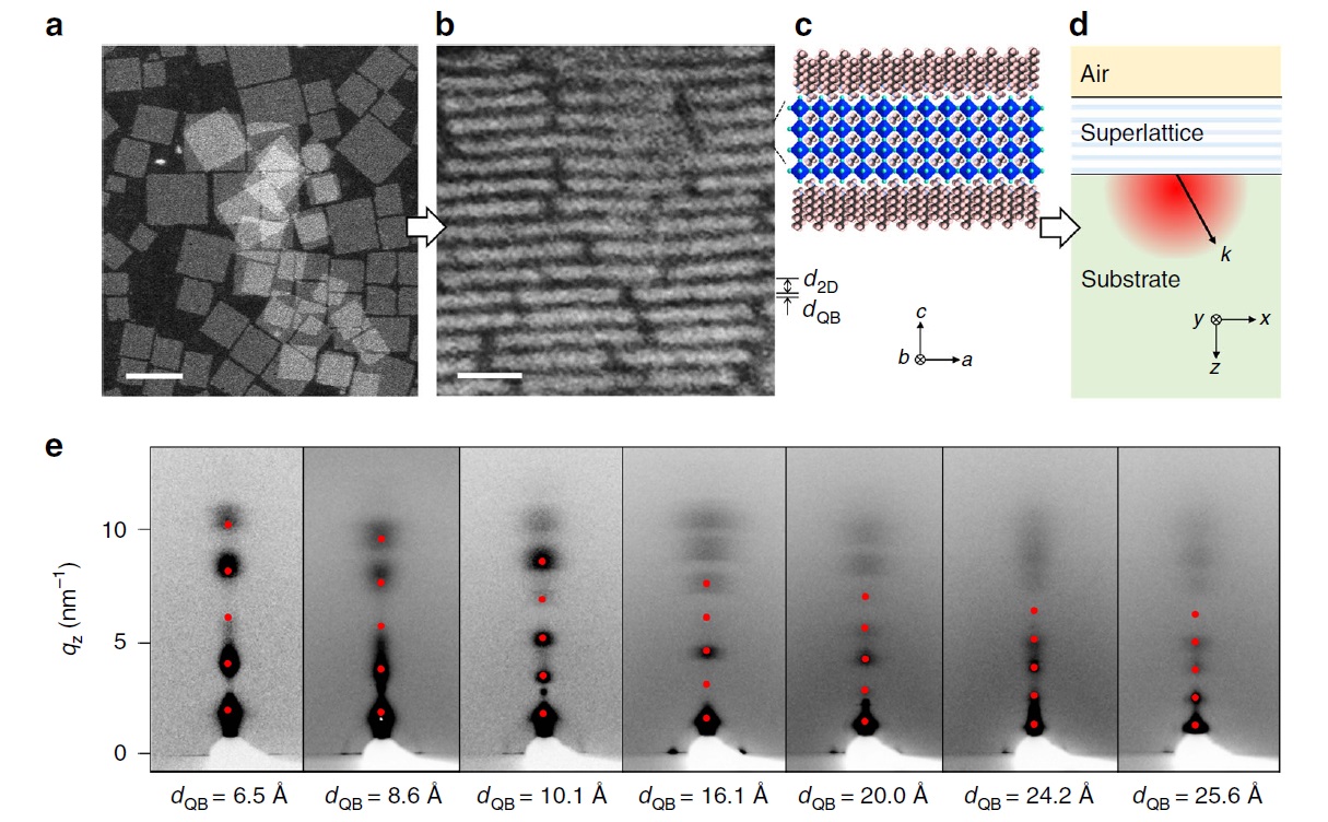
The MQW superlattices of 2D lead halide perovskites: Representative transmission electron micrographs of synthesized CQW nanocrystals (a; scale bar: 50 nm) and the cross sectional view of the fabricated MQW superlattice (b; d2D = 24.0 and dQB = 10.1 Å; scale bar: 10 nm). c The computer generated schematic of lattice structure (color code: cyan, bromine; pink, hydrogen; brown, carbon; and blue, nitrogen). d The superlattice in the Miller coordinate (a, b, c) is deposited on a transparent substrate forming the air/superlattice/substrate dielectric stack. Upon excitation, the emission with the wave vector k with respect to the space coordinate (x, y, z) is characterized (right). e The GIWAXS diffractograms for the fabricated superlattices. The red dots correspond to the calculated superlattice (0 0 l) peak positions according to the c axis perpendicular to the x–y plane up to five orders, giving the superlattice d-spacing, d2D + dQB. As d2D is 24 Å, the dQB values were quantified accordingly.
|
Very energy-efficient blue light
Using this process, the researchers have produced light sources for blue, green, yellow and orange light. They say that the red color component, which is also required for screens, cannot yet be realized with the new technology.
In the case of the newly created blue light, around two-fifths of the light generated reaches the eye of the observer, compared to only one-fifth with conventional QLED technology. “This means that our technology requires only half as much energy to generate light of a given intensity,” Professor Shih says. For other colors, however, the efficiency gain achieved so far is smaller, so the scientists are conducting further research with a view to increasing this.
Compared to conventional LEDs, the new technology has another advantage, as the scientists emphasize: the novel stacked QLEDs are very easy to produce in a single step. It is also possible to increase the intensity of conventional LEDs by arranging several light-emitting layers on top of each other; however, this needs to be done layer by layer, which makes production more complex.
 |
MQW superlattices with tunable emission wavelength
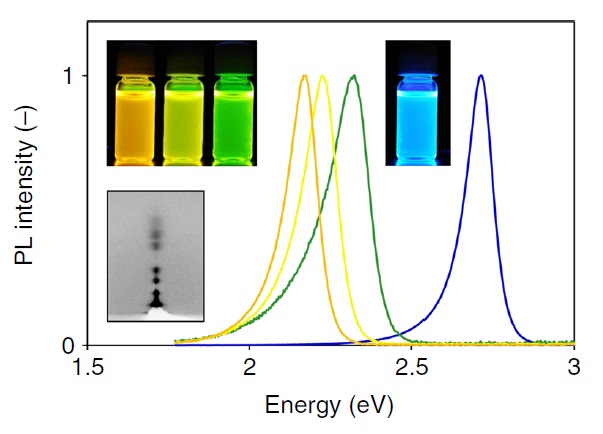
PL spectra for the as-prepared bromide (blue), and the mixed-iodide (green, yellow, and orange) CQWs. The photographs of solutions under UV excitation and the GIWAXS pattern for the green superlattice are shown in insets. |
Platelets instead of spheres make screens more economical
QLED screens have been on the market for a few years now. They are known for their bright, intense colors, which are produced using what is known as quantum dot technology: QLED stands for quantum dot light emitting diode. Researchers at ETH Zurich have now developed a technology that increases the energy efficiency of QLEDs. By minimizing the scattering losses of light inside the diodes, a larger proportion of the light generated is emitted to the outside.
Conventional QLEDs consist of a multitude of spherical semiconductor nanocrystals, known as quantum dots. In a screen, when these nanocrystals are excited from behind with UV light, they convert it into colored light in the visible range. The color of light each nanocrystal produces depends on its material composition.
However, the light these spherical nanocrystals emit scatters in all directions inside the screen; only about one-fifth of it makes its way to the outside world and is visible to the observer. To increase the energy efficiency of the technology, scientists have been trying for years to develop nanocrystals that emit light in only one direction (forward, towards the observer) – and a few such light sources already exist. But instead of spherical crystals, these sources are composed of ultra-thin nanoplatelets that emit light only in one direction: perpendicular to the plane of the platelet.
If these nanoplatelets are arranged next to each other in a layer, they produce a relatively weak light that is not sufficient for screens. To increase the light intensity, scientists are attempting to superimpose several layers of these platelets. The trouble with this approach is that the platelets begin to interact with each other, with the result that the light is again emitted not only in one direction but in all directions.
- Jagielski, J., Solari, S.F., Jordan, L. et al. Scalable photonic sources using two-dimensional lead halide perovskite superlattices. Nat Commun 11, 387 (2020) doi:10.1038/s41467-019-14084-3
- https://shihlab.ethz.ch/lise-news/lab-news/2020/01/nature-commun-scalable-photonic-sources-using-two-dimensional-lead-halide-perovskite-superlattices.html
- https://ethz.ch/en/news-and-events/eth-news/news/2020/01/qled-platelets-instead-of-spheres-make-screens-more-economical.html